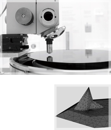
Customized MEMS structures and solutions:
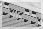
High aspect structures
3D-structures with high aspect ratio for microoptics or - fluidics.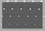
Flat nano-electrodes
A variety of metal electrodes with sizes down to 100 nm.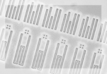
Active elements
Several active elements made of SiN or SiO2.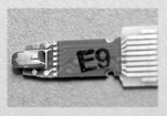
Thermal probe
Packaged probe with integrated thermal sensor.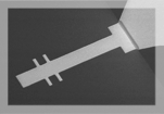
Spray coating structure
Resist structure at the bottom of a v-groove (depth ~280 µm).
Active arrays
Cantilever with integrated piezoresistive stress gauge (doped silicon).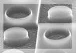
Grating
Grating suitable for the calibration of measurement tools (SEM, AFM).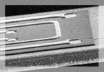
Elec. circuit on Si-bridge
Deflection sensor on a silicon bridge.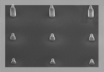
Spiked electrodes
Small EBD-grown spikes e.g. to measure biosignals.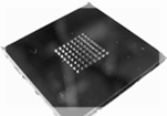
Metal membrane
Small and large metal membranes for nanopore filters.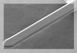
Si-Cantilever
Cantilevers made of silicon or nitride for any sensor application (e.g. func-tionalization).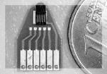
Magnetostrictive sensor
Detection of the bending by using the magnetostrictive effect (NiFe or NiCo).
AFM probe
Probes made of different materials suitable for Atomic Force Microscopes.
Adressable Si-chips
Arrays of individual addressable microstructures.
Perforated membrane
Thin Silicon membranes with holes down to 70nm in diameter.