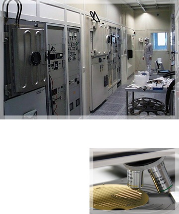
We have access to a large variety of manufacturing technologies which can be offered to our customers. Our process engineers enjoy broad experience in the set up and manufacturing of customized MEMS solutions.
In cooperation with the Fraunhofer IISB and the University Erlangen-Nürnberg the following single step processing tools are available:
100mm / 150mm Wafer Fab Capabilities:
Substrates
![]() Wafers of silicon, SOI (100mm), fused silica (100mm) and glass (100mm)
Wafers of silicon, SOI (100mm), fused silica (100mm) and glass (100mm)
![]() Experience in handling thin wafers and fragile structures
Experience in handling thin wafers and fragile structures
Lithography
![]() Laser Lithography (high resolution)
Laser Lithography (high resolution)
![]() Contact 1:1
Contact 1:1
Minimum features: ~0.8 µm (vacuum contact mode) or ~3 µm (proximity mode)
Alignment accuracy: ~0.5 µm (front side align), or ~2 µm (back side align)
Double-side lithography capabilities
![]() Photoresist coater (Resist thickness: 1-10 µm)
Photoresist coater (Resist thickness: 1-10 µm)
![]() Spray coating (Resist thickness: 1-10 µm)
Spray coating (Resist thickness: 1-10 µm)
![]() Positive and negative photoresist
Positive and negative photoresist
![]() Lift-off
Lift-off
Plasma Etching
![]() DRIE
DRIE
![]() Polysilicon
Polysilicon
![]() Metals (Al, AlSiCu, …)
Metals (Al, AlSiCu, …)
![]() Oxide ICP
Oxide ICP
Plasma Deposition
![]() PECVD nitride (LF/HF)
PECVD nitride (LF/HF)
![]() PECVD silicon oxide
PECVD silicon oxide
Wafer Bonding
![]() Anodic bonding (Alignment accuracy for wafer pairs < 5 µm, all bonding can be done in controlled ambient conditions or vacuum)
Anodic bonding (Alignment accuracy for wafer pairs < 5 µm, all bonding can be done in controlled ambient conditions or vacuum)
Furnace Processes
![]() Wet oxidation
Wet oxidation
![]() Dry oxidation
Dry oxidation
![]() Annealing processes
Annealing processes
![]() Doping processes (ion implantation)
Doping processes (ion implantation)
![]() Low-stress LPCVD nitride
Low-stress LPCVD nitride
![]() LPCVD oxides
LPCVD oxides
![]() LPCVD polysilicon
LPCVD polysilicon
Wet Etching
![]() Anisotropic silicon etching (KOH)
Anisotropic silicon etching (KOH)
![]() Wet etching of dielectrics (i.e. different oxides and nitrides)
Wet etching of dielectrics (i.e. different oxides and nitrides)
![]() Wet cleaning process; acid- and solvent based
Wet cleaning process; acid- and solvent based
![]() Wet etching of metals
Wet etching of metals
Metallization
![]() Sputter deposition (Al, Cr, Ni, Ti, PtIr)
Sputter deposition (Al, Cr, Ni, Ti, PtIr)
![]() Evaporation (Al, Au, Cr, Ni, Ti, Ag, Pd, Pt, Mo, Cu)
Evaporation (Al, Au, Cr, Ni, Ti, Ag, Pd, Pt, Mo, Cu)
Focused Ion Beam (FIB)
![]() Nano-structuring, cross-section analysis, electronic chip modification
Nano-structuring, cross-section analysis, electronic chip modification
Metrology
![]() SEM (+EDX)
SEM (+EDX)
![]() SPM (AFM, TUNA, SSRM, SCM, MFM, EFM, KPM)
SPM (AFM, TUNA, SSRM, SCM, MFM, EFM, KPM)
![]() Ellipsometer / Spectral ellipsometer
Ellipsometer / Spectral ellipsometer
![]() Inspection microscopes
Inspection microscopes
![]() Surface profiler
Surface profiler
![]() Sheet resistance (four-point probe)
Sheet resistance (four-point probe)
![]() Optical layer thickness measurement with spectral photometer
Optical layer thickness measurement with spectral photometer
![]() Vibration analyzer
Vibration analyzer